AND gate can be designed by using two simple diodes. The circuit driving voltage V is applied to the parallely connected diodes and the output is collected as the voltage drop at the diodes. In logic gates, the terms high voltage level means +5 V and low logic level means 0 V or ground.
When one of the inputs of the AND gate is connected to logic HIGH and other is connected to logic LOW then the diodes are at reverse bias condition and no voltage drop at the output. So the output is measured as LOW. If the two inputs are connected to LOW level input, then also the diodes will turn to reverse biased condition and allows no current. So again the output is measured as 0.
But when the two inputs (two diodes) are connected to a HIGH voltage level, then the two diodes are in forward biased condition (diodes switches are ON) so the output of the AND gate is HIGH, and measured as logic 1.

Outline
ToggleAND gate Logic Symbol and Boolean expression
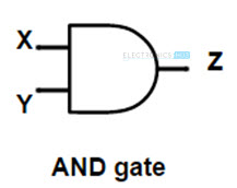
The AND gate is logically represented as shown below with two inputs and one output.
Boolean expression
If the inputs of the AND gate is X, Y and the output is Z then the operation of AND gate is mathematically expressed in the Boolean expression as Z = X. Y. This means the AND gate produces the multiplication of its inputs.
Truth table
The truth table for logical AND gate is given below.

The truth table describes us that the output of AND gate will be LOW with all combinations of inputs except for both high inputs condition.
Explanation of AND gate with light switch circuit
The AND gate switching circuit will have two inputs with two manually toggled switches. Let the two switches be A and B, then the we can explain the switching operation of AND gate as
- When both switches A and B are open (switches are supplied with low level input signal) i.e. A=0, B=0, then the bulb will not glow.
- When switch A is close (supplied with high level input signal) and B is open (supplied with low level input signal) i.e. A=1, B=0, then the bulb will not glow.
- When switch A is open (supplied with low level input signal) and B is close (supplied with high level input signal) i.e. A=0, B=1, then the bulb will not glow.
- When both switches A and B are close (switches are supplied with high level input signal) i.e. A=1, B=1, then the bulb will glow.
This operation of AND gate as light switching circuit is described in below pictures

Pulsed operation
If we apply two different clock signals the inputs of AND logic gate X and Y, then if we observe the output, it will be as shown below (X, Y are inputs and Z is output)
When both inputs are high, the output of the AND gate is also high and when either of the inputs is low, then the output comes to low level. At the end of the clock pulses in the above diagram, the output is at low level as both the inputs are low.
AND gate using BJT Transistors
We can design an AND gate by using diodes and transistors. The AND gate with BJT transistors is shown in below diagram.
Transistor switches are faster than diode switches. Similar to OR gate, we connect +6 V supply to both the transistors (to their collectors) through resistors. The emitter of the first transistor is connected to collector of the second and the emitter of second transistor is grounded by a resistor.
The output of the resistor is collected across the emitter and grounded resistor of the second transistor. The output of the AND gate is high only when the two transistors are conducting (at high voltage level) and at rest of input voltage combinations, the output is low.
3-Input AND gate
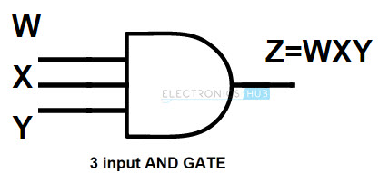
We can design an AND gate with 3 inputs also. Though the AND gate have 3 inputs, the Boolean equation will not change. Th output of the AND gate is equal to the sum of the inputs.
3-Input AND gate symbol
Truth table
The truth table of 3 –input AND gate is given below
The output of the 3 input AND gate is HIGH when all the 3 inputs are low and it will be LOW for all other combinations of inputs.
Multi-input AND Gate
AND gate mathematically produces the output equal to the multiplication of inputs. The operation is defined by “.” (a Dot). We can design n input AND gate by cascading the other AND gates as its inputs. Commercially, there is only 2 -input, 3 -input and 4 -input AND gate ICs are available. If we need additional inputs, we have to cascade the additional AND gates at the inputs of ICs.
For sample, here we design a 6 –input AND gate in below diagram.
The Boolean expression of 6 input AND gate is Q = (A.B). (C.D). (E.F). We can also design the odd numbered input AND gates by making some of the input pins as “unused”, by connecting them directly to Ground.
Commonly available TTL and CMOS logic AND gate IC’s
Complete list of AND gate ICs is given below
| 4019 | Quad AND-OR Select Gate |
| 4073 | Triple 3 -input AND gate |
| 4085 | Dual 2 -wide, 2 -input AND/OR invert (AOI) |
| 4086 | Expandable 4-wide, 2-input AND/OR invert (AOI) |
| 741G08 | single 2 -input AND gate |
| 7409 | quad 2 -input AND gate with open collector outputs |
| 741G09 | single 2-input AND gate with open drain output |
| 7411 | triple 3-input AND gate |
| 7415 | triple 3-input AND gate with open collector outputs |
| 7421 | dual 4-input AND gate |
| 7450 | dual 2-wide 2-input AND-OR-invert gate |
| 7451 | dual 2-wide 2-input AND-OR-invert gate |
| 7452 | expandable 4-wide 2-input AND-OR gate |
| 7453 | expandable 4-wide 2-input AND-OR-invert gate |
| 7454 | 4-wide 2-input AND-OR-invert gate |
| 7455 | 2-wide 4-input AND-OR-invert Gate |
| 7458 | 2-input and 3-input AND-OR Gate |
| 7459 | 2-input and 3-input AND-OR-invert Gate |
| 74130 | quad 2-input AND gate buffer with 30 V open collector outputs |
| 74131 | quad 2-input AND gate buffer with 15 V open collector outputs |
| 74808 | hex 2-input AND drivers |
| 741G3208 | single 3 input OR-AND Gate |
Among those all ICs, we use only some for our general applications. They are listed below.
TTL Logic AND Gates CMOS Logic AND Gates
74LS08 Quad 2-input CD4081 Quad 2 -input
74LS11 Triple 3-input CD4073 Triple 3 -input
74LS21 Dual 4-input CD4082 Dual 4 –input
7408 Quad 2-input AND Gate IC
The IC 7408 is used as a Quad 2 –input AND gate IC. The IC diagram is shown below. Let’s have a look
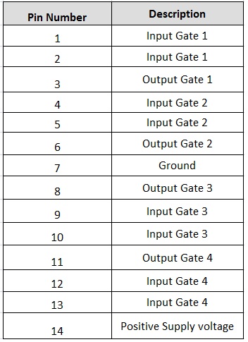
7408 is a TTL series AND gate. It has 4 AND gate in it. Each pin and its purposes of 7408 IC are explained below.
Pin description

Pin 14 is supplied with the maximum input of 5.2 volts D.C. If the supply voltage increases 5.2 Volts then the IC may damage due to high supply.
IC 4081
The IC 4081 is used as a Quad 2 –input AND gate IC. The IC diagram is shown below. It is a CMOS (complementary MOSFET) AND gate IC. Like TTL AND gate IC 7048, this CMOS AND gate IC has also 4 AND gates in it. Now let’s understand the internal pin diagram of IC 4081.
Pin description
The pin description of CMOS 4081 AND gate IC is explained below
Here too, Pin 14 is supplied with the maximum input of 5.2 volts D.C. If the supply voltage increases 5.2 Volts then the IC may damage due to high supply. Though the TTL AND gate IC and CMOS AND gate IC have same number of AND gates implemented in it, they differ in internal circuit arrangement.
AND gate Applications
Logic AND gate is used in many of the application s in our day to day life. Some of them are explained below.
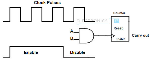
1) AND gate is used as Enable and Disable purpose on counter devices. If we observe the below circuit, when the counter starts counting from 0 to 100. When a counter receives the clock signal, then it increments its count by 1.
To make the counting operation successful from 1 to 100, counter circuit has to receive the pulses continuously. So the counter circuit can be controlled by the clock signal input at the input of counter. When we connect the clock signal as an input for 2 –input AND gate and the second input of the AND gate is connected to Disable/ Enable signal. We can stop the device counting by setting the second input to 0.
We know that when any one of the inputs is low, then the output of AND gate will become low (0). So if we apply the low level signal, 0 to the Enable /Disable pin, the output of the AND gate will be low, thus it doesn’t allow any clock signal.
So the clock signal doesn’t reach the counter so that we can stop the counting operation by making one of the inputs of the AND gate to low. If we want to start the counting again, we apply a high input at the enable/disable pin, i.e. it is set to 1. In this way the counter (its counting operation) is controlled by an AND gate.
2).The logic AND gate is used in some sort of security devices like garden flood-lights and security lights etc. They have a heat- radiation sensitive device called “Passive Infra- Red device (PIR)”. So when a hot object such as intruder (unauthorized entries like neighbor’s pets) is detected by the device, the heat sensor produces a high voltage making it to set in logic 1.
As the light of flood- light did not clearly visible in day time these devises comes in use, when the surroundings /atmosphere is dark. It comes to ON state when the heat sensor is triggered. The block diagram this security system with AND gate is shown below.
The mono -stable device produce only a single pulse when it is triggered. When the output of AND gate becomes high, then the output of the mono –stable device also goes high and hold for some interval of time. Transducer is used to provide enough current for the flood light.
As the flood light is a high voltage device, the output produced by the mono- stable device is not enough to drive the light. So we use a transducer to boost the current.
In commercial security devices, we use a Relay as a switch to ON and OFF the flood light.


